2007-06-18
1、What's IC packing?
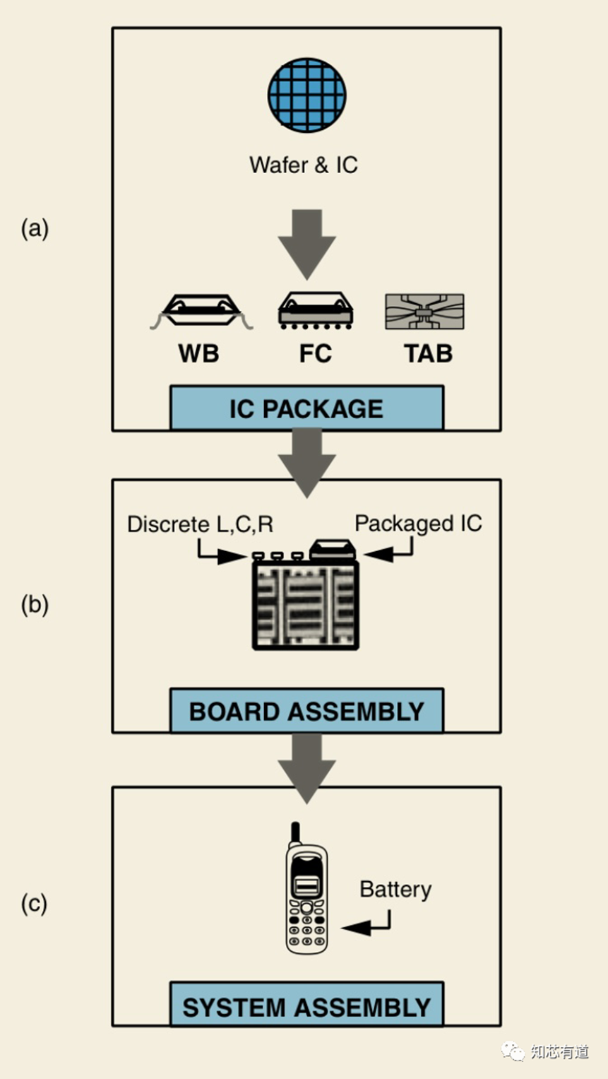
The diagram below depicts the entire process from wafer formation to the system. The most important step in this process is the packaging of the IC.

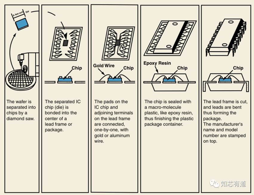
The function of an IC package is to protect, power, and cool these microelectronic devices, as well as to provide an electrical and mechanical connection between the components and the outside world. Each chip has its own unique packaging process, but for the sake of discussion, the diagram below shows a common process for a dual in-line package (DIP).

DIP was the first complex packaging solution developed shortly after the invention of ICs in the 1960s. Since then, a number of packaging solutions have been developed, but continue to be used even four years after their initial introduction due to their low cost and high reliability.
Packages are typically independent of IC manufacturing. When the IC or die is ready for packaging, it is bonded to the package. The input/output (I/O) connection pads on the IC are connected to the corresponding pads on the package by using gold or aluminum wire bonding. I/O is the connection that brings electrical signals to and from the chip. Once the die is wire-bonded to the package, the entire structure is sealed or molded with a plastic material such as epoxy. Only the package terminals or pins are visible to the outside, and everything else is completely sealed. Once the IC is sealed, the package is labeled with the manufacturer's name, model number, and other identifying information.
2、Packing classification

With so many IC types and IC requirements, it is impractical to have a single packaging solution for all ICs. To solve this problem, many types of IC packaging technologies have been developed, which differ in structure, materials, manufacturing methods, bonding techniques, size, thickness, number of I/O connections, heat dissipation capacity, electrical performance, reliability, and cost. Generally speaking, IC packages can be divided into two categories: 1) through-hole packages and 2) surface mount.
These two categories refer to the methods used when assembling packages into printed wiring boards (PWBs). If a package has pins that can be inserted into a PWB hole, it is called a through-hole package. If the package is not inserted into the PWB, but is mounted on the surface of the PWB, it is called a surface-mount package.
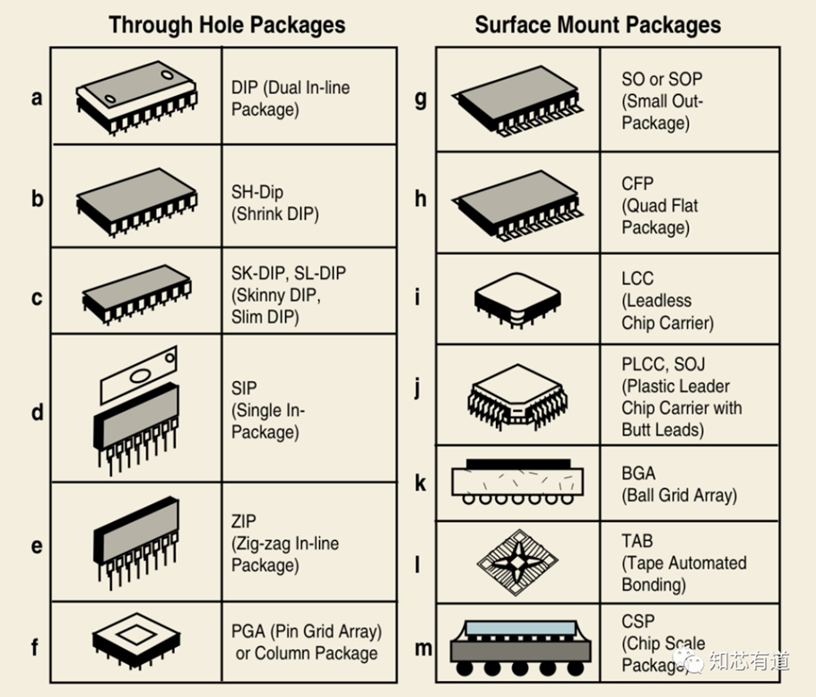
The advantage of surface-mount packages compared to through-hole is that both sides of the PWB can be used, so higher packing densities can be achieved on the board. These two types of packages are shown in the figure below.

Dual in-line packages (DIPs) and pin grid arrays (PGAs) are through-hole packages. In DIP, the I/O or pins are distributed on the sides of the package. To enable more I/O connections, the pins use PGAs in a regional array below the surface of the package. Most of the advancements and changes can be observed in surface mount packages.
Due to its extremely low cost, the small outline (SO) package is the most widely used package for low I/O applications in modern memory. The Quad Flat Pack (QFP) is an extension of the SOP with greater I/O connectivity. Both SOP and QFP have leads that can be connected to the PWB. There are also leadless packages such as LCC and PLCC, but their use is very limited. In the late 1980s, packages with solder balls were developed as an alternative to packages with leads. Solder balls can be placed below the surface of the package in the form of an array of zones and significantly increase the number of I/Os in a surface-mount package. Ball Grid Array (BGA) packages are an example of this technology. In the modern era of portable and handheld products, smaller, thinner, and lighter packaging is required. Chip Scale Packages (CSPs) have been developed to meet these needs of modern electronics. For example, DIP in the 1960s was about 100 times the size of the chip. Since then, developments in packaging technology have reduced the ratio of package area to die area by a factor of 4 to 5. By definition, a CSP is a package with an area smaller than 1.2 times the area of its package IC.

Contact: Miley
Phone: 0755-88266575
Email: info@mil-ic.com
Add: Room 2709,Block C,Xintian CBC Business Center,Shixia North Second Street,Futian District,Shenzhen,Guangdong,China